

The Hidden Power Drain in 1S Battery Laptops – and How to Fix It

Single-cell (1S) battery laptops are having a moment. By cutting the battery pack down to one cell instead of two or three in series, OEMs can lower system BOM cost and simplify the power architecture — fewer cells to balance, fewer protection components, and a lighter, thinner design overall. It’s no surprise more thin-and-light and budget-friendly laptops are adopting this approach.

But the 1S architecture comes with a catch that doesn’t show up on a spec sheet until you start measuring battery life: the LED backlight driver for the LCD display becomes noticeably less efficient. The reason is straightforward. A 1S cell sits at a lower voltage than a 2S or 3S pack, which means the boost converter driving the LED backlight has to work across a much larger voltage conversion ratio to reach the LED string voltage. Bigger conversion ratios mean bigger losses — and on a single cell, there’s nowhere for that inefficiency to hide.

This problem is getting worse, not better, for an ironic reason: the rest of the system is improving. SoCs, memory, and other platform components keep getting more power-efficient, especially in low-power standby modes. As those components shrink their share of total power draw, the display — and specifically the LED backlight driver — stands out even more. In many modern designs, the display now accounts for as much as 70% of total system power. What used to be one power consumer among many is now, by far, the biggest one.

That makes backlight driver efficiency a first-order design decision, not an afterthought. This is exactly where pSemi’s ARC1C0608 comes in. It’s purpose-built for this exact challenge:

  • Full 1S battery range support — it operates cleanly across the entire discharge curve of a single cell, from full charge down to cutoff, without efficiency collapsing at the low end.
  • Peak efficiency >94% — even with the larger conversion ratio inherent to 1S systems.
  • Parallel-able architecture — multiple ARC1C0608 devices can be combined to drive the higher LED currents needed for high-resolution, high-brightness displays, without sacrificing efficiency as brightness scales up.
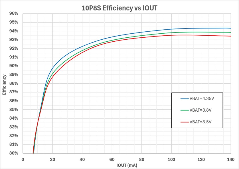
Figure 1. ARC1C0608 Efficiency vs IOUT in parallel operation

Figure 1 shows the 2pcs parallel ARC1C0608 efficiency in 10P8S LED configuration at different battery voltages. The peak efficiency is >94% with a very tight efficiency gap between different voltages.   

The efficiency number matters more than it might seem. Going from a typical competing solution to >94% efficiency roughly cuts backlight power losses in half. Since the backlight is now the single largest power draw in the system, that kind of loss reduction translates directly into real, noticeable battery life — often an extra hour of runtime with no other changes to the platform.

As 1S battery designs continue to spread across the laptop market, the LED backlight driver is quickly becoming the component that separates a good battery life story from a great one. Solutions like the ARC1C0608 show that you don’t have to trade off BOM savings and simplicity for runtime — with the right driver, you can have both.

Please visit https://psemi.com/products/power-management/led-boost-arc1c0608-arc1c0605/ to learn more about ARC1C0608.

Please contact Sales@psemi.com for any questions.

Markets

Power Management

Markets

  • RF Switches All

    Industry-leading linearity and RF performance
    HaRP™ technology enhancement reduces gate lag and insertion loss drift
    Monolithic CMOS solution that integrates RF, analog and digital
    Best-in-class ESD and reliability
  • High Linearity RF Switches

    Industry-leading linearity and RF performance
    HaRP™ technology enhancement reduces gate lag and insertion loss drift
    Monolithic CMOS solution that integrates RF, analog and digital
    Best-in-class ESD and reliability
  • High Isolation RF Switches

    Industry-leading isolation and RF performance
    HaRP™ technology enhancement reduces gate lag and insertion loss drift
    Monolithic CMOS solution that integrates RF, analog and digital
    Best-in-class ESD and reliability
  • Low Insertion Loss RF Switches

    Industry-leading insertion loss and RF performance
    HaRP™ technology enhancement reduces gate lag and insertion loss drift
    Monolithic CMOS solution that integrates RF, analog and digital
    Best-in-class ESD and reliability
  • Antenna Tuning Switches

    Industry-leading RF power handling and ruggedness
    Best-in-class harmonic and linearity
    Small form factor with robust ESD and reliability
  • 75Ω Wired Broadband Switches

    Unmatched linearity performance for DOCSIS 3.1
    HaRP™ technology enhancement reduces gate lag and insertion loss drift
    Monolithic CMOS solution that integrates RF, analog and digital
    Best-in-class ESD ratings and reliability
  • Broadband RF Switches

    Wideband support with a frequency range from 0 Hz to 67 GHz
    Industry-leading insertion loss, isolation, linearity and settling time
    HaRP™ technology enhancement reduces gate lag and insertion loss drift
    Best-in-class ESD and reliability
  • High Power Switches

    Industry-leading power handling and RF performance
    HaRP™ technology enhancement reduces gate lag and insertion loss drift
    Monolithic CMOS solution that integrates RF, analog and digital
    Best-in-class ESD and reliability
  • Automotive Switches

    AEC-Q100 Grade 2-certified supporting temperatures up to +105°C
    HaRP™ technology enhancement reduces gate lag and insertion loss drift
    Monolithic CMOS solution that integrates RF, analog and digital
    Best-in-class ESD and reliability
  • Extended Temperature RF Switches

    Wide temperature range support from -55°C to +125°C
    HaRP™ technology enhancement reduces gate lag and insertion loss drift
    Monolithic CMOS solution that integrates RF, analog and digital
    Best-in-class ESD and reliability
  • 75Ω Wired Broadband RF Digital Step Attenuators

    High linearity, fast switching time with wide bandwidth
    Best-in-class attenuation error with fine attenuation steps
    Monolithic CMOS solution that integrates RF, analog and digital
    Excellent ESD protection and reliability
  • Glitchless RF Digital Step Attenuators

    High linearity, fast switching time with wide bandwidth
    Best-in-class attenuation error with fine attenuation steps
    Monolithic CMOS solution that integrates RF, analog and digital
    Excellent ESD protection and reliability
  • General-purpose RF Digital Step Attenuators

    High linearity, fast switching time with wide bandwidth
    Best-in-class attenuation error with fine attenuation steps
    Monolithic CMOS solution that integrates RF, analog and digital
    Excellent ESD protection and reliability
  • 2.4 GHz IoT FEMs

    Industry-leading monolithic Wi-Fi RF front-end solutions
    High linearity performance for Wi-Fi 6 and W-Fi 6E
    Compact form factors integrating high-performance RF, analog and digital
    Best-in-class ESD and reliability
  • Phase Shifters

    Ideal solutions for optimizing transmission phase angle
    Low root-mean-square (RMS) phase and amplitude error with fine phase resolution
    Digital control interface with parallel and serial programming options
    Best-in-class ESD and reliability
  • Monolithic Phase & Amplitude Controllers (MPACs)

    Reliable phase and amplitude control for next-generation communications
    Monolithic CMOS solution that integrates RF, analog and digital
    Integrated solution for Doherty power amplifier optimization (MPAC–Doherty)
  • Digital Tunable Capacitors (DTCs)

    Small form factor with high Q
    Monolithically integrated impedance tuning solution
    Wide-band tuning coverage, minimum mismatch losses, high linearity and fast switching speed
    Best-in-class ESD and reliability
  • Power Limiters

    Highly integrated solutions, smaller and more reliable than PIN-diode solutions
    Adjustable threshold control for maximum design flexibility
    High power handling and linearity required for wide-dynamic-range designs
    Fast response and recovery times for instantaneous protection and rapid return
  • Prescalers

    Exceptional performance with high-frequency support up to 13.5 GHz
    Low phase noise performance and low power consumption solutions
    Bare-die solutions for a wide variety of compact high-performance applications
    Best-in-class ESD and reliability
  • Mixers

    Broadband quad MOSFET array cores for high performance
    Industry-leading linearity, isolation and low conversion loss
    Available in MSOP, DFN and QFN packages
    Best-in-class ESD and reliability
  • Switch LNA

    Integrates dual-channel LNA with bypass function & high-power switch
    20W average RF input power
    Low noise figure of 0.9 dB
    +105°C operating temperature
  • Charge Pump Capacitor Divider

    Unique, patented architecture to enable higher overall system, power conversion efficiency
    Fully integrated solutions from 15W to 160W
    Virtually lossless (up to 99% peak) conversion and soft-switching topology
    Parallel operation to higher power levels
    Available through our parent company Murata
  • 2-Stage Buck Regulators

    Family of DC-DC buck voltage regulators ICs and modules for telecoms, datacoms, server and storage applications
    Compact solution size offering best-in-class efficiencies for low profile applications (<1.2mm)
    Fully programmable via I2C and with accurate on-board telemetry
    Available through our parent company Murata
  • 2-Stage Boost Regulators - LED Backlight Drivers

    Ultra-high efficiency (up to 96%) LED boosts for LCD displays
    Product family includes products for 1-cell, 2-cell, and 3-cell inputs such as tablets, notebooks and 2-in-1 convertibles
    Enables very low profile (<0.7 mm) solutions and halves power-conversion losses compared to leading alternatives
    Up to 15-bit resolution via I²C or PWM control
    High accuracy with tight matching at low LED current
  • Multi-level Converters

    Industry-first 4-level and 3-level conversion for fixed input voltages (USB_PD)
    Configurable as charge pump divide-by-3 and divide-by-2 for variable input voltages (USB_PPS)
    Wide range input voltage 4.5V to 18V compatible with USB and wireless charging Qi sources
    Reverse boost capability
    High-accuracy current and voltage telemetry
    Best-in-class efficiency for low-profile applications (<1 mm)
    Targets fast-charging battery applications

Power Management

RF Mixers & Limiters

Front End Modules

RF Phase & Amplitude Control

Skip to content