
As compute density climbs—in AI accelerators, networking ASICs, and high-performance servers—the humble point-of-load (PoL) converter is under more pressure than ever. Boards are moving to 12V (and higher) bus voltages to cut distribution losses, but that shifts a heavier burden onto the final conversion stage that steps 12V down to the sub-1V rails modern silicon demands.
A charge pump (CP) placed ahead of the buck converter—as a fixed-ratio pre-regulator, typically dividing 12V down to 6V or 4V—has emerged as one of the most effective ways to solve this. This article explains why it matters.
1. Higher efficiency, better thermal budget, more headroom for performance
A switched-capacitor charge pump moves the charge using capacitors instead of inductors, so it avoids the resistive and core losses that dominate a traditional buck stage at high step-down ratios. Splitting the conversion into a CP pre-regulator (12V→6V, ~98%+ efficient) followed by a buck (6V→VCORE) lets each stage operate near its efficiency sweet spot, rather than forcing a single buck to survive a brutal 12:1 or higher ratio.
The system-level payoff is straightforward: every watt not burned as heat is a watt available for compute. Lower losses mean a cooler power stage, which frees up thermal margin— margin that system architects can reallocate toward higher clock speeds or higher core counts within the same power and cooling envelope. In power-constrained platforms, efficiency isn’t just an OpEx line item, it’s a performance lever.
2. Smaller x-height—critical for vertical power delivery
Charge pumps are capacitor-dominated rather than inductor-dominated. Because capacitors (especially MLCCs) are inherently lower profile than the power inductors a comparable buck stage would need, a CP pre-regulator stage can be built noticeably thinner.
his matters most in vertical power delivery (VPD) architectures, where power stages sit directly beneath the processor package to shorten current paths and minimize IR drop. Z-height is at a premium in these designs—every extra millimeter under the socket affects socket-to-heatsink clearance and overall system stack-up. Swapping bulky inductors for low-profile capacitors in the pre-regulation stage ensures that VPD designs hit their height targets without compromising current delivery.
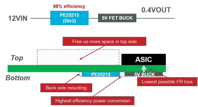
Figure 1: Using CP for low-profile vertical power delivery
3. Lower input-to-output ratio speeds up load transient response
Buck converter transient response is fundamentally tied to duty cycle and step-down ratio. A buck regulating straight from 12V to ~0.8V operates at a very low duty cycle, which limits how quickly the inductor current can slew in response to a sudden load step—exactly the scenario modern processors create with aggressive dynamic power states.
By inserting a charge pump ahead of the buck, the buck must now only convert from an intermediate rail—such as 6V—down to VCORE. That lower input-to-output ratio raises the effective duty cycle, which directly improves the buck’s control-loop bandwidth and transient response. The result is tighter voltage regulation during fast load transients—less droop, less overshoot, and a reduced need for oversized output capacitance compensate.
4. Enables low-voltage FETs in the buck stage
Because the buck converter now sees a much lower input voltage—6V or 4V instead of 12V—it can use lower-voltage-rated power FETs. Lower-voltage FETs typically have significantly lower on-resistance RON and gate charge for a given silicon area, which further reduces conduction and switching losses in the buck stage. This compounds with benefit #1: the CP’s efficiency gain plus the buck’s own efficiency improvement from using the low-voltage FETs stack to deliver a meaningfully more efficient overall power delivery network.
5. Lower EMI, smaller filter, lower BOM cost
Charge pumps switch large amounts of charge without the sharp di/dt and inductive ringing associated with inductor-based converters, resulting in inherently lower electromagnetic interference. Lower EMI at the CP stage—combined with the buck now operating at a lower input voltage and smaller step-down ratio—reduces the filtering burden across the power path.
Practically, this means that fewer and smaller input/output filter capacitors are needed to meet EMI and ripple targets. That translates directly to board space savings and lower bill-of-materials cost, both of which matter enormously at scale.
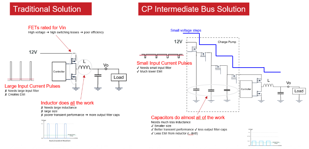
Figure 2: Comparison between traditional 12V PoL and CP intermediate-bus PoL
6. pSemi PE25213: a purpose-built CP for 12V PoL
Among available charge pump solutions, the pSemi PE25213 stands out as particularly well-suited to 12V PoL applications. Key differentiators include:
- ~99% efficiency peak efficiency, minimizing the loss penalty of adding a conversion stage.
- Selectable DIV2/DIV3 modes, giving designers the flexibility to tune the intermediate rail (6V or 4V) to best match their downstream buck’s optimal operating window and FET voltage rating
- Dynamic mode switchover: in the event of an input power loss or sag, the PE25213 can switch from DIV3 to DIV2 mode. This raises the intermediate rail on the fly, helping the downstream buck avoid tripping into an under-voltage protection (UVP) fault during a power-loss transient—a critical resilience feature for systems that can’t tolerate unplanned shutdowns.
7. Conclusion
As 12V PoL systems push toward higher currents, tighter transient specs, and denser vertical power delivery, the two-stage CP + buck architecture is becoming less of a nice-to-have and more of a necessity. By offloading the bulk of the step-down ratio to a highly efficient, low-profile charge pump, designers can unlock system-level efficiency gains, faster transient response, smaller BOM, and lower EMI—all while giving the downstream buck room to use lower-voltage, more efficient FETs. Devices like the pSemi PE25213, with its selectable DIV2/DIV3 modes and dynamic switchover protection, are purpose-built to make this architecture practical and robust for next generation 12V PoL designs.