

Taking Mobile Charging to the Next Level: How Multi-level Power Conversion is Reshaping Smartphone Design

As smartphones become thinner and faster, and AI drives more power-hungry processors and higher battery capacity, power management engineers face an increasingly difficult challenge: deliver more charging power and higher efficiency without consuming valuable space inside the device. 

pSemi, a Murata company and leader in advanced power management solutions, unveiled the PE26100breakthrough multi-level buck regulator architecture designed for nextgeneration mobile platforms. Combining high-efficiency power conversion, support for wired and wireless charging standards, and an ultra-low-profile design under 1 mm, this innovation addresses some of the industry’s most pressing power delivery challenges. 

More importantly, it represents a fundamental shift in how power conversion can be implemented in mobile electronics. 

As shown in Figure 1, a typical smartphone architecture uses a main interface PMIC with some level of charging capability – usually relatively low current. To increase charging speed and reduce charging time, the PE26100 multi-level converter is added as a parallel or auxiliary charger. 
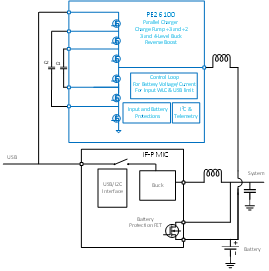
Figure 1: Typical smartphone charging systems with PE26100 as the auxiliary charger providing fast charge to complement the main charger. 

The Challenge: More Power in Less Space

Modern smartphones have become extraordinarily complex systems. Engineers must fit processors, batteries, antennas, cameras, sensors, memory, RF subsystems, and charging electronics into increasingly compact form factors. Every cubic millimeter matters. 

At the same time, user expectations continue to rise. Consumers expect faster battery charging, longer battery life, and higher performance from AI-enabled processors and advanced mobile applications. These trends place significant demands on power delivery systems. 

Traditional buck converters have served the industry well for decades. They efficiently stepdown voltage from a power source to the lower voltages needed by batteries and processors. However, conventional buck architectures require larginductors with high z-height. 

For ultra-thin smartphones and tablets, these larger magnetic components can become a major design constraint. 

Why Multi-level Conversion Matters

Multi-level buck conversion addresses this challenge by increasing the number of switching voltage levels available within the converter. 

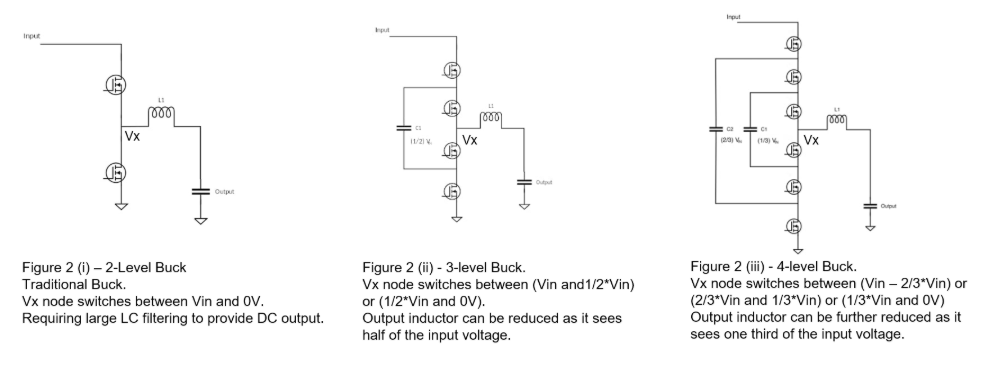
In a traditional buck converter (Figure 2(i)), the switching node alternates between just two levels: input voltage and ground. In contrast, a 3-level converter (Figure 2(ii)), introduces an additional voltage state, while a 4-level converter (Figure 2(iii)), introduces four levels. 

This architectural change delivers significant benefits. 

By reducing the voltage excursion seen at the switching node, multi-level converters dramatically lower inductor ripple current. Additionally, the inductor sees twice the switching frequency of the FETs. As a result, designers can use smaller, lower-profile inductors while maintaining high power capability. 

The architecture also reduces voltage stress on switching MOSFETs. In a 3-level converter, MOSFETs experience only half the input voltage. In a 4-level converter, they experience just one-third. 

Lower voltage stress allows the use of lower-voltage MOSFETs with significantly lower on-resistance (RDS(on)), reducing conduction losses, and improving efficiency. 

The result is a power converter that delivers high current while reducing component size and improving overall system performance 
A Flexible Architecture for Modern Charging Standards

One of the most significant challenges facing smartphone manufacturers today is supporting multiple charging ecosystems. 

Devices must accommodate USB Power Delivery (USB-PD), Programmable Power Supply (PPS), and wireless charging standards such as Qi, and numerous regional charging implementations. Input voltages can vary dramatically depending on the charging source. 

pSemi’s PE26100 hybrid multi-level architecture was designed specifically to address this challenge. 

The converter operates across an exceptionally wide 4.5 V to 18 V input range, enabling compatibility across modern charging technologies. Depending on operating conditions, the architecture intelligently adapts its topology – switching between regulated, multi-level, buck modes and switching-capacitor, chargepump modes, as follows:

  • 4-level buck mode for higher input voltages. 
  • 3-level buck mode for mid-range voltages. 
  • Divide-by-2 capacitor-divider mode for low-voltage PPS operation. 
  • Divide-by-3 capacitor-divider mode for higher-voltage PPS operation. 

This creates what can best be described as an intelligent hybrid converter. This adaptability allows a single power conversion platform to support a diverse charging ecosystem while maintaining high efficiency. 

For smartphone manufacturers, this can simplify system design and improve charging performance regardless of whether power arrives from a wired USB-PD adapter, a PPS charger, or a wireless charging pad. 

Built for Fast Charging and AI Processing

Beyond battery charging, modern mobile systems increasingly require high-current power delivery for advanced AI processing. 

As semiconductor technologies continue moving toward smaller process nodes, operating voltages decrease while current requirements rise. Advanced mobile processors often demand substantial electrical current delivered with tight regulation and minimal losses. 

The pSemi architecture is designed with these requirements in mind. 

Each device can deliver up to 6 A of current while using a low-profile 1mm inductor. Multiple devices can also be paralleled to support even higher power levels and faster charging applications. 

This capability makes the technology well suited for battery charging future generations of AI powerhungry smartphones. 

From Research to Real-world Product Innovation

While multi-level conversion concepts have existed in higher-voltage industrial and power applications for years, bringing them into the highly constrained mobile environment required significant innovation. 

Challenges such as fly capacitor balancing, control complexity, and switching-state management had to be overcome before a practical mobile solution could emerge. 

Drawing on more than a decade of research and intellectual property development, including foundational work originating from MIT patents, pSemi has successfully translated these concepts into a commercial platform optimized for mobile electronics. 

The result is what pSemi describes as the industry’s first multi-level converter capable of operating in both 4-level buck mode and high-current capacitor-divider charge pump configurations. In short, pSemi is not simply improving battery charging. It is redefining how power is converted, managed, and delivered in the mobile devices of tomorrow. 

Markets

Power Management

Markets

  • RF Switches All

    Industry-leading linearity and RF performance
    HaRP™ technology enhancement reduces gate lag and insertion loss drift
    Monolithic CMOS solution that integrates RF, analog and digital
    Best-in-class ESD and reliability
  • High Linearity RF Switches

    Industry-leading linearity and RF performance
    HaRP™ technology enhancement reduces gate lag and insertion loss drift
    Monolithic CMOS solution that integrates RF, analog and digital
    Best-in-class ESD and reliability
  • High Isolation RF Switches

    Industry-leading isolation and RF performance
    HaRP™ technology enhancement reduces gate lag and insertion loss drift
    Monolithic CMOS solution that integrates RF, analog and digital
    Best-in-class ESD and reliability
  • Low Insertion Loss RF Switches

    Industry-leading insertion loss and RF performance
    HaRP™ technology enhancement reduces gate lag and insertion loss drift
    Monolithic CMOS solution that integrates RF, analog and digital
    Best-in-class ESD and reliability
  • Antenna Tuning Switches

    Industry-leading RF power handling and ruggedness
    Best-in-class harmonic and linearity
    Small form factor with robust ESD and reliability
  • 75Ω Wired Broadband Switches

    Unmatched linearity performance for DOCSIS 3.1
    HaRP™ technology enhancement reduces gate lag and insertion loss drift
    Monolithic CMOS solution that integrates RF, analog and digital
    Best-in-class ESD ratings and reliability
  • Broadband RF Switches

    Wideband support with a frequency range from 0 Hz to 67 GHz
    Industry-leading insertion loss, isolation, linearity and settling time
    HaRP™ technology enhancement reduces gate lag and insertion loss drift
    Best-in-class ESD and reliability
  • High Power Switches

    Industry-leading power handling and RF performance
    HaRP™ technology enhancement reduces gate lag and insertion loss drift
    Monolithic CMOS solution that integrates RF, analog and digital
    Best-in-class ESD and reliability
  • Automotive Switches

    AEC-Q100 Grade 2-certified supporting temperatures up to +105°C
    HaRP™ technology enhancement reduces gate lag and insertion loss drift
    Monolithic CMOS solution that integrates RF, analog and digital
    Best-in-class ESD and reliability
  • Extended Temperature RF Switches

    Wide temperature range support from -55°C to +125°C
    HaRP™ technology enhancement reduces gate lag and insertion loss drift
    Monolithic CMOS solution that integrates RF, analog and digital
    Best-in-class ESD and reliability
  • 75Ω Wired Broadband RF Digital Step Attenuators

    High linearity, fast switching time with wide bandwidth
    Best-in-class attenuation error with fine attenuation steps
    Monolithic CMOS solution that integrates RF, analog and digital
    Excellent ESD protection and reliability
  • Glitchless RF Digital Step Attenuators

    High linearity, fast switching time with wide bandwidth
    Best-in-class attenuation error with fine attenuation steps
    Monolithic CMOS solution that integrates RF, analog and digital
    Excellent ESD protection and reliability
  • General-purpose RF Digital Step Attenuators

    High linearity, fast switching time with wide bandwidth
    Best-in-class attenuation error with fine attenuation steps
    Monolithic CMOS solution that integrates RF, analog and digital
    Excellent ESD protection and reliability
  • 2.4 GHz IoT FEMs

    Industry-leading monolithic Wi-Fi RF front-end solutions
    High linearity performance for Wi-Fi 6 and W-Fi 6E
    Compact form factors integrating high-performance RF, analog and digital
    Best-in-class ESD and reliability
  • Phase Shifters

    Ideal solutions for optimizing transmission phase angle
    Low root-mean-square (RMS) phase and amplitude error with fine phase resolution
    Digital control interface with parallel and serial programming options
    Best-in-class ESD and reliability
  • Monolithic Phase & Amplitude Controllers (MPACs)

    Reliable phase and amplitude control for next-generation communications
    Monolithic CMOS solution that integrates RF, analog and digital
    Integrated solution for Doherty power amplifier optimization (MPAC–Doherty)
  • Digital Tunable Capacitors (DTCs)

    Small form factor with high Q
    Monolithically integrated impedance tuning solution
    Wide-band tuning coverage, minimum mismatch losses, high linearity and fast switching speed
    Best-in-class ESD and reliability
  • Power Limiters

    Highly integrated solutions, smaller and more reliable than PIN-diode solutions
    Adjustable threshold control for maximum design flexibility
    High power handling and linearity required for wide-dynamic-range designs
    Fast response and recovery times for instantaneous protection and rapid return
  • Prescalers

    Exceptional performance with high-frequency support up to 13.5 GHz
    Low phase noise performance and low power consumption solutions
    Bare-die solutions for a wide variety of compact high-performance applications
    Best-in-class ESD and reliability
  • Mixers

    Broadband quad MOSFET array cores for high performance
    Industry-leading linearity, isolation and low conversion loss
    Available in MSOP, DFN and QFN packages
    Best-in-class ESD and reliability
  • Switch LNA

    Integrates dual-channel LNA with bypass function & high-power switch
    20W average RF input power
    Low noise figure of 0.9 dB
    +105°C operating temperature
  • Charge Pump Capacitor Divider

    Unique, patented architecture to enable higher overall system, power conversion efficiency
    Fully integrated solutions from 15W to 160W
    Virtually lossless (up to 99% peak) conversion and soft-switching topology
    Parallel operation to higher power levels
    Available through our parent company Murata
  • 2-Stage Buck Regulators

    Family of DC-DC buck voltage regulators ICs and modules for telecoms, datacoms, server and storage applications
    Compact solution size offering best-in-class efficiencies for low profile applications (<1.2mm)
    Fully programmable via I2C and with accurate on-board telemetry
    Available through our parent company Murata
  • 2-Stage Boost Regulators - LED Backlight Drivers

    Ultra-high efficiency (up to 96%) LED boosts for LCD displays
    Product family includes products for 1-cell, 2-cell, and 3-cell inputs such as tablets, notebooks and 2-in-1 convertibles
    Enables very low profile (<0.7 mm) solutions and halves power-conversion losses compared to leading alternatives
    Up to 15-bit resolution via I²C or PWM control
    High accuracy with tight matching at low LED current
  • Multi-level Converters

    Industry-first 4-level and 3-level conversion for fixed input voltages (USB_PD)
    Configurable as charge pump divide-by-3 and divide-by-2 for variable input voltages (USB_PPS)
    Wide range input voltage 4.5V to 18V compatible with USB and wireless charging Qi sources
    Reverse boost capability
    High-accuracy current and voltage telemetry
    Best-in-class efficiency for low-profile applications (<1 mm)
    Targets fast-charging battery applications

Power Management

RF Mixers & Limiters

Front End Modules

RF Phase & Amplitude Control

Skip to content